What's inside a BLE COVID test?
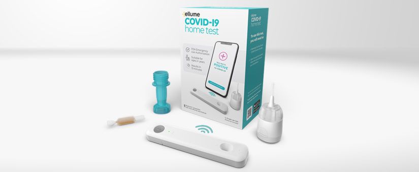
This week for some extra peace of mind, my friend let me use one of their spare rapid tests prior to visiting with them later in the day. With the Omicron variant rampaging around, it seemed like a wise precaution on top of us both being vaccinated/boosted.
This particular test works in conjunction with a smartphone app. After connecting the "analyzer" to the app, you drop your sample in a small hole. 15 minutes later, the app displays the test result.
After the test had given me my negative result, I decided to disassemble the analyzer
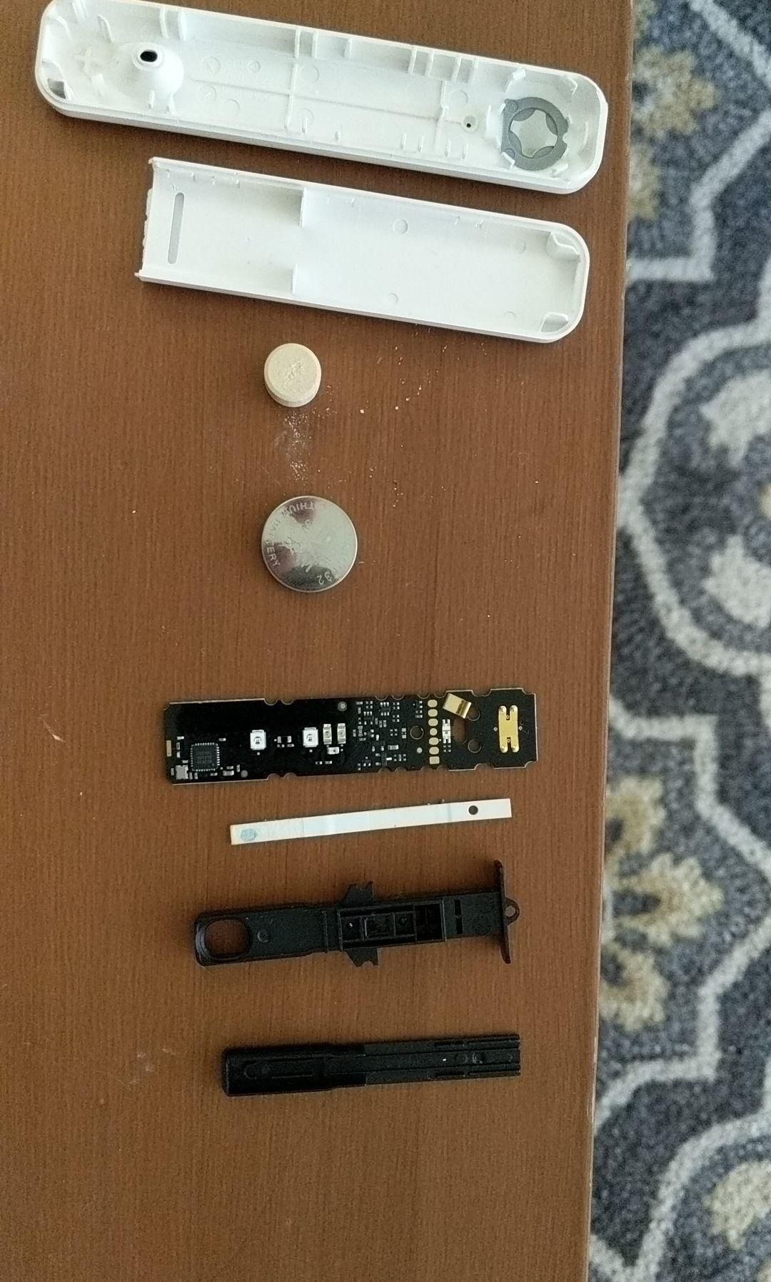
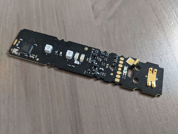
The white strip, normally mounted above the PCB, is the COVID-relevant part. This is a seemingly typical lateral flow test strip, positioned such that the end is under the sample-accepting hole. On the other side not pictured are a pair of pregnancy test-style lines. Presumably one shows blue to indicate the test is valid, while the other indicates a positive result when visible. There are some lights and sensors on the PCB aligned with these areas on the strip.
I am tempted to label this another instance of IoT-gone-mad, but maybe this one is potentially justifiable, given high stakes and low cost of powerful electronics, if you absolutely want to remove human error from the equation?
The white round pill-like object appears to be some kind of moisture absorber, which makes sense; the analyzer (and its contained strip) is kept in a sealed bag prior to use.
The QFN32 chip on the left of the PCB is where the magic happens - a Nordic Semiconductor nRF52810. This is a BLE-capable microcontroller with GPIO and some internal peripherals including a temperature sensor. I figured it'd be a fun exercise to try to reprogram the device, perhaps to make a bluetooth temperature sensor or beacon, or something similar. Encouragingly, there are a bunch of nRF52-based boards on Adafruit with complete Arduino-compatible firmware, including parts to drive the BLE radio; hopefully that will not be difficult to leverage here.
I did some poking around with a multimeter, hoping the set of 7 pads near the right end of the PCB was a programming port of some kind. This turned out to be the case, and the 3-wire ARM "SWD" (Serial Wire Debug) port, or "SW-DP" can be found here.
The meanings of each pad, specifically:
1. GND
2. ?
3. ?
4. VDD
5. SWDIO
6. SWCLK
7. Reset
I couldn't find the meaning of #2 and #3 without more poking than I felt like doing for now, though it might come up later.
The MCU has integrated power conditioning/regulation, and there's no obvious external regulator. There's what is probably a P-channel MOSFET between the battery + and VDD. When the analyzer is powered down the gate is pulled high, seemingly to avoid draining the battery via leakage current while not in use.
Though it's physically awkward to verify, the sole button on the device probably holds this gate low when pressed, powering up the MCU. The firmware then likely engages some GPIO to keep the gate low after the button has been released. The MCU can then release that when it decides to power itself off.
While the device is powered up, the button is held down to initiate some 'pairing' with the smartphone app, so I expect there's some extra circuitry that permits the state of the button to be read via a separate GPIO.
I ordered an open source JTAG interface which seems to be nRF52 compatible, glancing at the github repo. I've used such products rarely and could be missing some obvious reason this won't work, but so far it's looking positive. The code in the repo also shows that there's support for the MCU's ERASEALL command via the CTRL-AP or Control Access Port. Confusingly, this is internally referred to as "erase_mass"; this will be needed for writing new code, if it turns out the MCU's program memory is protected.
I'll keep thinking about possible applications for this, and when the JTAG interface arrives in the mail I can actually try some stuff.